TOP > NSK Tribology Collaborative Research Cluster
 |
Prof. Tadahiko SHINSHI | |
| Room: R2 | Mail-Box: R2-38 | |
| TEL: 045-924-5095 | ||
| E-mail: shinshi.t.ab(at)m.titech.ac.jp Please replace “(at)” with “@”. |
||
| HomePage: http://www.nano.pi.titech.ac.jp/ | ||
 |
 |
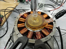
| Centrifugal blood pump using bearingless slice motor | |
 |
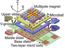 |
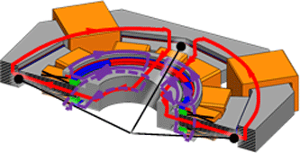
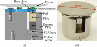
| Ultra-high response steering mirrors for laser scanning | 2-DOF MEMS linear motor |

|
Prof. Satoshi MOMOZONO(Specially Appointed)〔Shinshi Lab〕 |
|
| Room: G3 | Mail-Box: G3-1 | |
| TEL: 045-924-5956 | ||
| E-mail: momozono.s.aa(at)m.titech.ac.jp Please replace “(at)” with “@”. |
||
| HomePage: https://nsktrib-en.labby.jp/ | ||
・Tribological phenomena in rolling machine elements
・Contact mechanics of rough surfaces
・Surface
properties, wettability
・Friction and wear of elastomers
・Tribology in Biology and Ergonomics
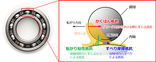
Tribological phenomena in rolling machine elements
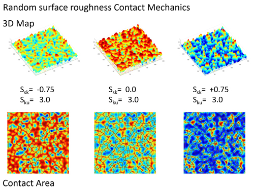
Contact mechanics of rough surfaces
国立大学法人東京科学大学
総合研究院 未来産業技術研究所
Laboratory for Future Interdisciplinary Research of Science and Technology (FIRST),
Institute of Integrated Research (IIR),
Institute of Science Tokyo
Copyright (C) Institute of Science Tokyo. All rights reserved.